
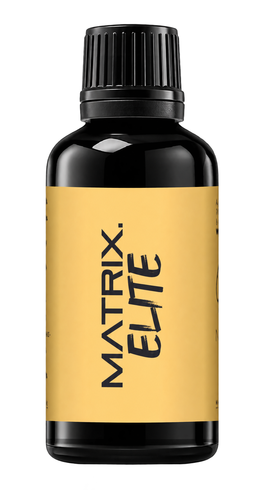
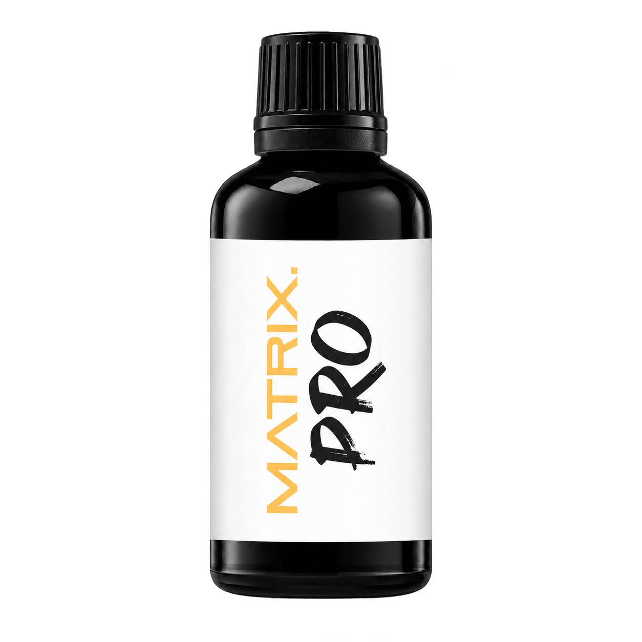
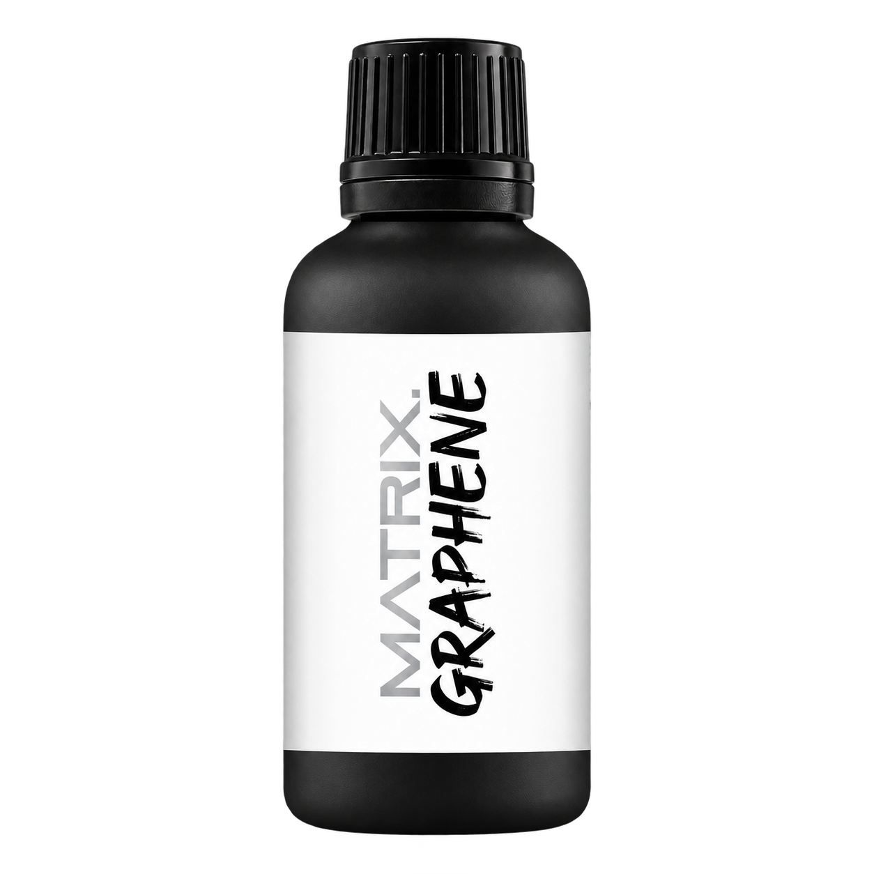
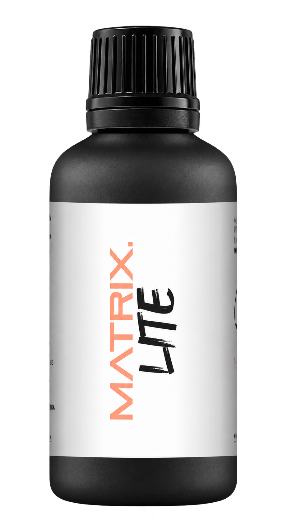


A full polishing range.
From cutting and one-step correction to final finishing.
Specialist chemistry. Expert application.
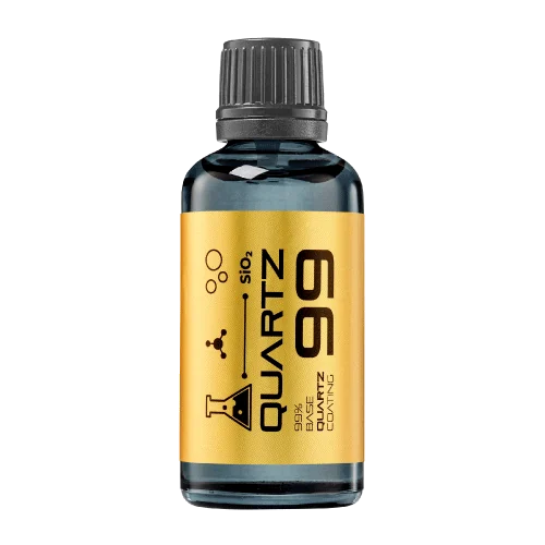 QUARTZ99 / CERAMIC BASE COAT
The foundation of your coating system.
A layerable quartz base coat designed for mechanical protection. Pair it with a suitable top coat to create the final finish.
For application by NANOLAB certified installers only.
Four formulas. Extended working time. Find the coating for your finish.
Explore the BEAST family of ceramic coatings.
Find the coating for each exterior surface.
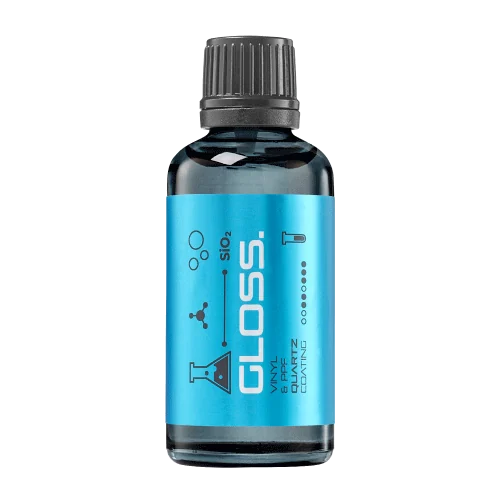 PPF & VINYLGLOSSProtection for glossy films and wraps.Discover
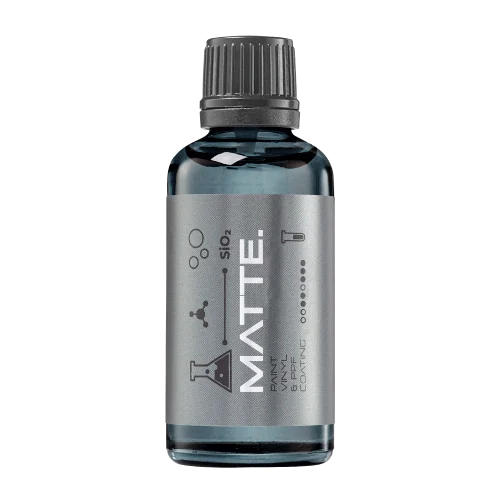 MATTE & SATINMATTEProtection that respects the finish.Discover
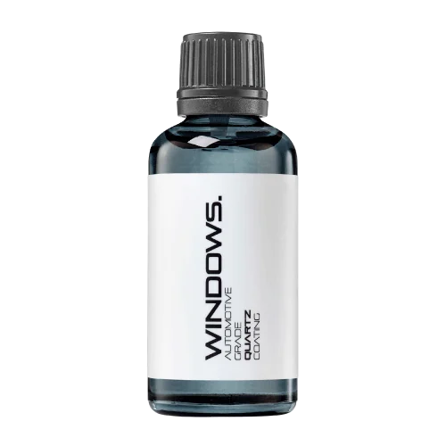 GLASSWINDOWSExplore dedicated glass protection.Discover
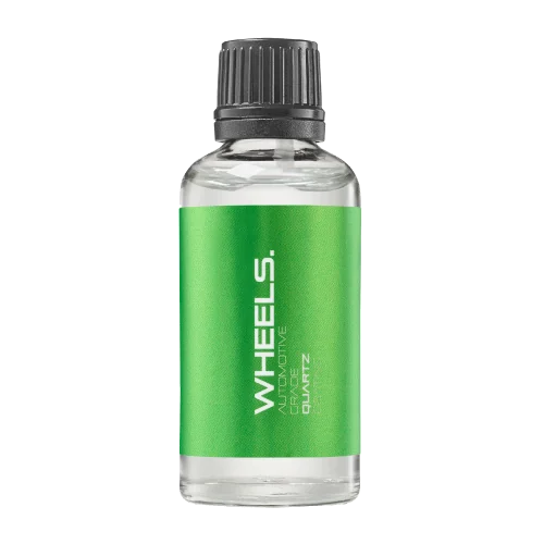 WHEEL PROTECTIONWHEELSA dedicated coating for your wheels.Discover
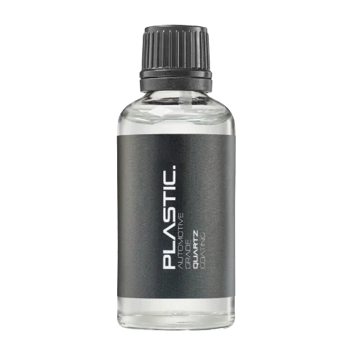 TRIM PROTECTIONPLASTICProtection for plastic surfaces.Discover
Dedicated care for the surfaces inside.
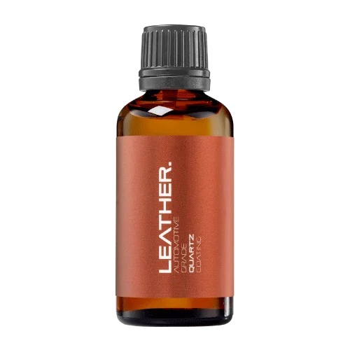 LEATHER SURFACESLEATHERDiscover NANOLAB leather protection.Discover PLASTIC SURFACESPLASTICProtection for interior plastic surfaces.Discover TEXTILE SURFACESFABRICExplore the latest fabric formulation.Discover
Spray protection, maintenance and upcoming wash products.
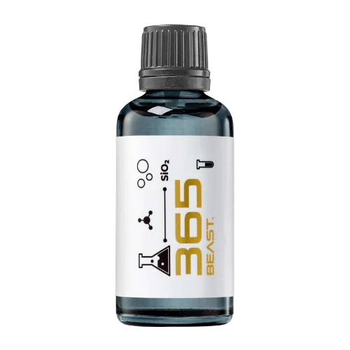 MAINTENANCEBEAST 365Explore the BEAST maintenance range.Discover
Next in washing, cleaning & care.
Ceramic protection for boats and yachts.
An easy-to-apply ceramic coating with an established track record on boats and yachts around the world.
Results vary with surface preparation, exposure and maintenance.
Read 50 MARINE guides →Explore MARINEProtection for the surfaces you live with.
A look at what we’re developing.
From cutting and one-step correction to final finishing.
A wider range for professional vehicle care.
Taking shape alongside BEAST & MATRIX.
Practical guidance for your next coating project.
Explore all guides →
A stripe along the edge of a compounding section may be excess residue, incomplete coverage or a different amount of repeated work.
Updated · NANOLAB Knowledge
A stripe along the edge of a compounding section may be excess residue, incomplete coverage or a different amount of repeated work. Before polishing the stripe again, determine which of those conditions is present. The section boundary is part of the process, not a place that can be ignored during inspection.
Remove product using a compatible method and a fresh towel. Inspect whether the stripe changes with cleaning. Residue pushed to the perimeter can look like a correction difference even when the underlying surface is consistent.
If the stripe remains, compare it with the working map. Did adjacent sections meet, overlap or leave a gap? Were some passes extended beyond the planned boundary while others stopped short? The cleaned pattern can reveal coverage differences, but starting damage must also be considered.
Choose a small area spanning the boundary and inspect both sides under the same light. Identify whether the remaining issue is original scratches, cutting haze or texture variation. Do not automatically use heavy compound on a boundary that only needs appropriate refinement.
Where rework is justified, define the new working area and the intended outcome. Avoid repeatedly chasing a moving stripe outward across the panel. Clean and inspect once the limited correction is complete.
Use visible panel landmarks or a diagram to establish manageable sections. Follow a consistent pass pattern with appropriate overlap for the selected system. Keep the section size within the operator’s controlled reach and the product’s working conditions.
Record completed areas separately from accepted areas. A panel that has been touched by the machine is not necessarily ready for the next stage. Include section junctions in the acceptance check rather than inspect only the easiest central patch.
The objective is consistent appearance across the whole panel. A fast series of individually attractive test squares is not sufficient if their boundaries remain visible after the product film is removed.
For current NANOLAB product instructions and compatibility, visit product documentation or contact the technical team.